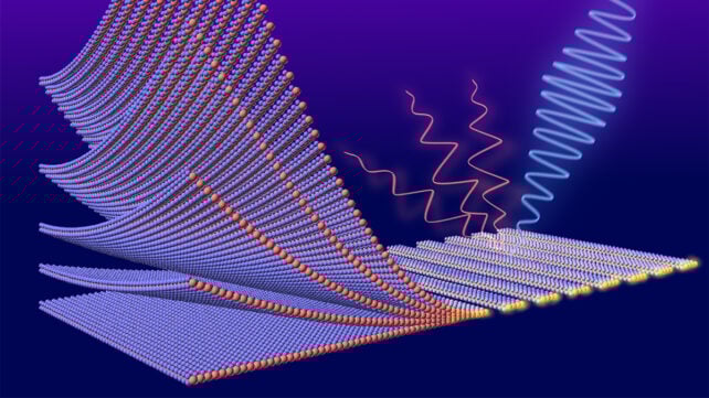
Scientists have managed to trap beams of infrared light in a lattice of specially engineered atoms that's just 42 nanometers thick. That's around 2,000x thinner than a human hair or an even thinner sliver of a standard sheet of paper.
The impressive feat, led by a team from the University of Warsaw in Poland, promises significant implications for light-based electronics, as technology components continue to become smaller and more precise.
It's also a notable advance in the study of infrared light, which has longer wavelengths than visible light. Being able to trap infrared light in tiny spaces is a challenge that can push the constraints of physics.
"The presented results are promising for the realization of flat, ultracompact devices for lasing, wavefront control, and higher-order topological states of the light," write the researchers in their published paper.
The key to the experiment carried out here lies in the material used for the grating that holds the light in place. It's made from layered atoms of molybdenum and selenium, creating an ultra-thin molybdenum diselenide (MoSe2) structure.
That special chemical construction maximizes the grating's refractive index, its ability to bend and slow down light (ready for trapping).
While MoSe2 has long been known to have a high refractive index, manufacturing it reliably at the smallest scales has previously proved problematic.
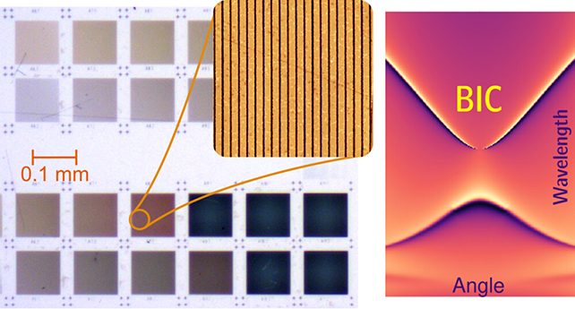
In this new study, the researchers used an atomic 'printing' method known as molecular beam epitaxy (MBE) to create MoSe2 sheets. As well as growing the sheets, the researchers also carved microscopic stripes into them – with gaps smaller than the wavelength of infrared light (subwavelength) – ready to hold photons in place.
One more physics trick was required for this to work, called a "bound state in the continuum" (BIC). It's a phenomenon where, in this case, light waves are confined within a material despite coexisting with other waves that radiate away.
To create a BIC, the materials for it need to be precisely designed and configured, which the researchers ensured by carefully modeling the MoSe2 grating before building it.

"We exploited the exceptionally high refractive index of MoSe2 to innovatively design and produce MoSe2-based subwavelength gratings hosting BICs," write the researchers.
There are some potential real-world applications of this complex physics. Scientists continue to explore the idea of optical computing – where photons of light replace electrons and electricity – which could significantly improve processing speeds while reducing component size.
While many hurdles remain before optical computing can become viable, demonstrations like the one detailed here show that it may be possible to trap and manipulate light with the necessary degree of precision – and at the tiniest scales.
In terms of this specific material and light trap, more work is needed before it can be reliably rolled out at scale. The sheet-growing process the team came up with wasn't perfect, so the material was polished with silk tissues to remove inconsistencies.
However, the researchers are confident that their approach can be developed further and even expanded into other areas.
MoSe2 belongs to a larger family of super-thin materials called transition metal dichalcogenides (TMDs), and the hope is that new ways can be found to produce and manipulate TMDs more reliably.
That would pave the way for gadgets that are even smaller and faster than the ones we have today, built in part by trapping light in incredibly small spaces.
Related: Light Waves Brought to a Stop in a Crystal Promises New Ways to Control Photons
"The ease and simplicity of processing MoSe2 confirm that other designs of photonic structures, such as 2D metasurfaces based on TMD layers, are feasible," write the researchers.
The research has been published in ACS Nano.