In what could be the development that keeps Moore's law plugging along, scientists in the US have produced a transistor that's just a few atoms thick, opening up the possibility of some ridiculously tiny electronics.
First proposed in 1965, Moore's law predicts that the overall processing power of computers will double every two years, and while it's still pretty much accepted as a rule, people have started to doubt its longevity. Surely there's a limit to how many transistors we can pack into an integrated circuit? Well, if there is, it looks like we haven't hit it yet, because a team from Cornell University in the US have achieved a pretty significant record with their new tiny transistor.
The transistor is made using two-dimensional semiconductors known as transition-metal dichalcogenides (TMDs). When reduced to a single layer, these TMDs are just three atoms thick, made from members of a family of elements called transition metals. One of these, molybdenum disulfide, is a type of silvery, black metal that's been touted for its superior electrical qualities over the past few years.
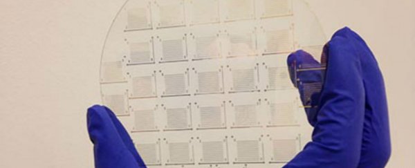
The team crystallised it down, and figured out how to peel ultra-thin sheets just a few atoms thick from the surface of the crystals. Amazingly, even at this thickness, the molybdenum disulfide film retained its electrical properties, which makes it a promising candidate for use in future electronics. "The electrical performance of our materials was comparable to that of reported results from single crystals of molybdenum disulfide, but instead of a tiny crystal, here we have a 4-inch (10-cm) wafer," one of the team, Jiwoong Park, said in a press release.
To create this atoms-thick molybdenum disulfide film, the team used a technique called metal organic chemical vapour deposition (MOCVD), which involves starting with a powdered form of the material, converting that into a gas, and sprinkling single atoms onto a substrate, one layer at a time.
"The process starts with two commercially available precursor compounds - diethylsulfide and a metal hexacarbonyl compound - mixed on a silicon wafer and baked at 550 degrees Celsius for 26 hours in the presence of hydrogen gas," explains Russell Brandom at The Verge. "The result was an array of 200 ultra-thin transistors with good electron mobility and only a few defects. Just two of them failed to conduct, leaving researchers with a 99 percent success rate."
Publishing in Nature, the team says the next step is to figure out how to produce the film in a more consistent way, so the conductivity can be more accurately measured. But what they've achieved so far is a real step in the right direction.
"Lots of people are trying to grow single layers on this large scale, myself among them," materials scientist Georg Duesberg from Trinity College Dublin in Ireland, who was not involved in the research, told Elizabeth Gibney at Nature. "But it looks like these guys have really done it."