There's no question that 3D printing is having a profound and sudden impact on society. Yet it's a field largely dominated by experts who have access to expensive systems that can generate accurate 3D scans of objects.
But this could soon be changing thanks to engineers at the California Institute of Technology, who have developed an inexpensive and super-compact 3D imaging device, which can be integrated into a smartphone.
With its device, the team says that scans of an object taken with a smartphone camera can be sent to a 3D printer, which will then produce a replica of the object, accurate to within a few micrometres of its original dimensions.
The device is known as a nanophotonic coherent imager, and is built onto an inexpensive silicon chip less than a square millimetre in size.
The team, which has described the device in the journal Optics Express, says it provides the highest depth-measurement accuracy of any such device ever created, and its key feature is the ability to infer depth.
In a regular smartphone camera, each pixel represents the intensity of the light received from a specific point in the image. The camera, however, can't determine how near or far away the object is.
By contrast, the nanophotonic 3D imager can gauge both light intensity and distance.
"Each pixel on the chip is an independent interferometer - an instrument that uses the interference of light waves to make precise measurements - which detects the phase and frequency of the signal in addition to the intensity," said Ali Hajimiri in a press release.
The chip uses a laser imaging technology called LIDAR, which lights up a target object with scanning laser beams. When these beams reflect off the object, the returning light is analysed based on the wavelength of the laser light used.
This process allows the chip's LIDAR system to accurately determine the object's size and its distance from the laser, ultimately building up a precise 3D model.
"By having an array of tiny LIDARs on our coherent imager, we can simultaneously image different parts of an object or a scene without the need for any mechanical movements within the imager," Hajimiri said.
One of the key developments of the technology was the miniaturisation of the LIDAR system.
"By coupling, confining, and processing the reflected light in small pipes on a silicon chip, we were able to scale each LIDAR element down to just a couple of hundred microns in size - small enough that we can form an array of 16 of these coherent detectors on an active area of 300 microns by 300 microns," Hajimiri said.
The team's first proof of concept has only 16 pixels, meaning that the 3D images it produces can only be 16 pixels at any given instance. But they've developed a nice work-around to image larger objects, doing so in four-pixel by four-pixel segments.
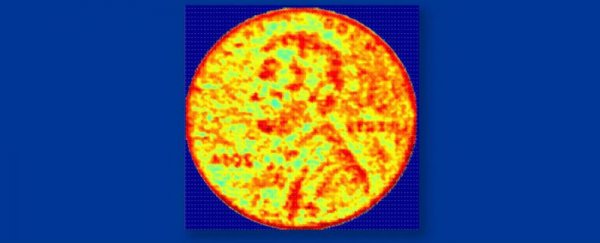
With this method, the team used the device to scan and create a 3D image of a coin with micron-level resolution from 50 cm away.
Hajimiri says the current array of 16 pixels could, in future, be scaled up to hundreds of thousands, and says these chips could find other applications, such as helping driverless cars avoid collisions.