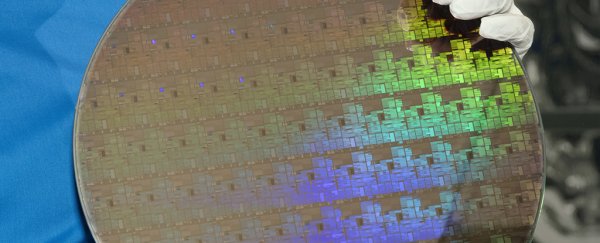
IBM researchers have announced a brand new way of manufacturing computer chips, one that will see 30 billion transistors packed into a space the size of a fingernail, and give a serious boost to the processing power we need.
Key to the innovation is halving the size of the transistor gates on current chips from 10 nanometres to 5 nanometres (nm) – more gates means more power and more efficiency, and that's going to help in everything from self-driving cars to smartphones.
To do this, IBM and partners Samsung and Global Foundries came up with a new design for future chips that overcomes some of the limitations of the current architecture. It's called FinFET, or Fin Field Effect Transistor.
"It's a big development," Dan Hutcheson, CEO of semiconductor firm and research publisher VLSI Research, told Brian Barrett at Wired. "If I can make the transistor smaller, I get more transistors in the same area, which means I get more compute power in the same area."
IBM is saying these chips will be 40 percent quicker with the same power draw, which means they will save 75 percent in power when running at the same speed as today's chips.
Imagine a phone processor that's as fast as the ones we have today, but only uses up a quarter of the same battery power in a day – that's the kind of improvement we're talking about.
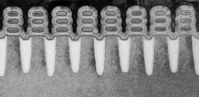 Cross-section view of the new 5-nm architecture. Credit: IBM Research
To improve on the FinFET architecture, which uses three current-carrying channels per transistor, researchers used a stacked silicon nanosheet design to effectively create another channel.
More channels allow for more current when the transistors are on, and faster leakage when the transistors are off, and that's where the power and efficiency gains come from.
In simple terms, the team has turned the FinFET architecture sideways, and stacked more transistors on top of each other.
This quest for faster and more efficient processors has been going on for as long as the technology has been around, and was summed up by the famous Moore's Law, put forward by Intel co-founder Gordon Moore in 1965.
Moore initially predicted that the number of transistors on a chip would double every year to keep powering faster and more efficient computers, then a decade later revised the prediction to every two years.
Things have been slowing lately, as progress struggled to hold to a prediction that was never intended to last so long. But engineers have used the idea as an incentive, striving to keep Moore's Law alive.
This new architecture IBM and its partners have come up with means we should be seeing big gains in computer chips for years to come.
It also enables engineers to use existing processes and materials rather than promising alternatives like carbon nanotubes, so our current technology can keep up with our needs while next-generation options are explored.
Production on 7-nm chips made using FinFET architecture is scheduled to start in 2018 and the brand new 5-nm chips could be ready a year or so after that, but don't expect to see them in consumer gadgets straight away.
With big jumps forward happening in artificial intelligence, data speeds, and many other areas, the race is on to process more data more quickly with less energy, and the new 5-nm chips should be a big help.
"The world's sitting on this stuff, artificial intelligence, self-driving cars," Hutcheson told Wired. "They're all highly dependent on more efficient computing power."
"That only comes from this type of technology. Without this, we stop."
The research will be presented at the the 2017 Symposia on VLSI Technology and Circuits in Kyoto, Japan.
Correction (7.06.2017): An earlier version of this story stated that the computer chips can fit 30 million transistors; this has now been changed to the correct scale of 30 billion. We regret the error.