You only need to take a look at the hefty mainframes of the 1950s and 1960s to understand how quickly computers and electronics have been miniaturised, but there's room for them to go smaller still, if this new research is any indication. Scientists have come up with a new chip fabrication approach that they say could lead to much thinner and flexible computer chips in the future.
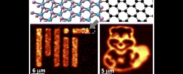
Developed by a team at MIT, it's the first chip fabrication technique where significantly different materials are deposited in the same layer. Today's computer chips, in contrast, are built from (very thin) layers stacked on top of one another, with precise patterns etched into them. The researchers say they've refined the process far enough to be able to build chips containing "all the circuit components necessary to produce a general-purpose computer".
"The methodology is universal for many kinds of structures," says Xi Ling, one of the authors of the paper. "This offers us tremendous potential with numerous candidate materials for ultra-thin circuit design."
The layers of material are just 1-3 atoms thick, and they chose graphene as one of the materials used - the 'wonder material' has already been used in a variety of different innovations and experiments, and its thinness and strength makes it perfect for use in thin-film electronics.
In fact, the new process can mix any material that combines elements from group 6 of the periodic table (including chromium, molybdenum, and tungsten) and elements from group 16 (including sulphur, selenium, and tellurium). As many of these compounds are semiconductors - which form the basis of transistor design - they can prove very useful in extremely thin layers of electronics.
In the tests run by the MIT team, a layer of graphene is deposited on a silicon substrate, with gaps etched in for the second material to fill. This second material, molybdenum disulphide, is applied using a solid bar of material known as a PTAS. As the PTAS passes over the chip, its molecules cause a reaction with the exposed silicon, and a layer of molybdenum disulphide is formed. The same process can be used to combine several different materials in the same way.
While the science is tricky to wrap your head around, the eventual applications are simple: thinner, more flexible electronics that take new shapes, set new levels of portability, or attach themselves to other objects as a layer of film. The next step is to use the technology to try and create tunnelling-transistor processors, which use a quantum mechanical effect to block a charge or allow it through.
The work has been published in the journal Advanced Materials.
*Image above: The researchers used the MIT and Tim the Beaver logos to show photoluminescence emissions from a monolayer of molybdenum disulfide inlayed onto graphene. The arrow indicates the graphene-MoS2 lateral heterostructure, which could potentially form the basis for ultrathin computer chips.