Scientist have spotted a strange type of quantum movement occurring in electrons travelling between the atomic layers of a material.
Instead of travelling from the top to the bottom layer through the middle, the electrons were caught disappearing from the top layer and reappearing in the bottom letter a fraction of a second later - with no trace of them existing in between.
"Electrons can show up on the first floor, then the third floor, without ever having been on the second floor," said lead researcher Hui Zhao from the University of Kansas.
This bizarre phenomenon could be used to create entirely new 'van der Waals materials', that combine unique nanomaterials to produce handy new properties - and are hoped to one day offer a big boost to electronics and things like solar cells.
If van der Waals forces sound familiar to you, that's because they're the strange quantum forces that enable gecko feet to stick to walls.
But they also describe any kind of attractive forces between molecules that don't come from traditional ionic or covalent bonds.
In a very simplified nutshell, van der Waals forces are the result of quantum mechanical attractions between particles, rather than a regular attraction between a positive and a negative particle.
And in recent years, scientists have begun using these forces to create new materials by layering together different 2D structures without regular bonds.
But until now, very little has been known about how electrons travel through these van der Waals materials, and as a result, how useful they'll be for electronic applications.
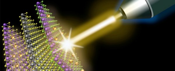
To figure this out, the researchers experimented with a van der Waals material that was made up of three 2D layers - similar to ultra-thin graphene - held together by van der Waals attractions.
The three layers the researchers tested were MoS2, WS2, and MoSe2 - all semiconducting materials, which means they can conduct electrons without resistance, and all of which respond to light with different colours.
That meant the researchers could use different coloured lasers to affect only electrons in one of the three layers, and not the others - and it allowed them to track where the electrons were travelling throughout the material.
To kick off the electrons, the team used an ultra-short laser pulse of just 100 femtoseconds (a femtosecond is one-quadrillionth of a second) to liberate some of the electrons in the top MoSe2 layer, so they could move freely.
"The colour of the laser pulse was chosen so that only electrons in the top layer can be liberated," said Zhao.
"We then used another laser pulse with the 'right' colour for the bottom MoS2 layer to detect the appearance of these electrons in that layer. The second pulse was purposely arranged to arrive at the sample after the first pulse by about 1 picosecond, by letting it travel a distance 0.3 mm longer than the first."
A picosecond is trillionth of a second, or around 1,000 femtoseconds.
The team found that the electrons moved from the top to the bottom layer of the material in that incredibly short time frame, taking just 1 picosecond to make the transition on average.
To figure out how they were getting there so quickly, they then used a third laser pulse with another colour to monitor the middle layer - and were surprised to find no electrons in there at all, defying regular physics.
"If electrons were things that followed 'common sense', like so-called classical particles, they'd be in the middle layer at some point during this one picosecond," said Zhao.
Thinking their result might have been a fluke, this bizarre quantum 'hopping' from the top to the bottom layer was further confirmed by simulations at the University of Nebraska-Lincoln.
The fact that it's shown up twice in two separate labs suggests that it's a real quantum phenomenon that lets electrons travel between atomic layers connected by van der Waals forces.
Further research is always needed to probe these new observed quantum phenomenon, but if verified, this is a good sign that van der Waals materials will be incredibly useful for electronics - and it's something that could be used to develop even more types of materials.
"This study showed electrons can transfer between these layers in a quantum fashion, just like in other conductors and semiconductors," said Zhao.
The research has been published in Nano Letters.